

Growth is good; no one in the semiconductor industry would argue this point. And according to Gartner, there’s a lot of “good” on the horizon. Current forecasts call for semiconductor sales to more than double in this decade, going from $400 billion in 2020 to $1T by 2030.
With growth, however, come growing pains. To reach the heights of $1T-plus in semiconductor sales, the industry must evolve by significantly increasing not only the amount of wafers and wafer starts annually but also the amount of investment in equipment and materials. Semiconductor materials consumption during the same decade is expected to double as well. This creates great opportunity for materials suppliers, but it also will mean taking a hard look at the materials supply chain – what are the challenges, and how can they be addressed?
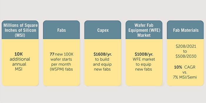
Figure 1: What does a $1T industry mean to the supply chain?
A key challenge will be aggressive capacity expansion across all material segments to support this fast semiconductor industry growth. Given the long cycle of investment and cyclical nature of semiconductor business, this is challenging and requires longer-term planning to execute. For materials developers, this growth will create new demands for higher purity and lower variability of your materials – which, in turn, will mean investing in tighter process controls and new approaches to materials packaging.
There are some fundamental realities of physics driving the need for purer materials. The semiconductor industry has continued to shrink device geometries, with some advanced chips already being manufactured at the 3nm node. This creates a very small margin of error for detection of truly minuscule killer defects. On-wafer inspection tools’ detection capabilities range from 10-15nm, so it falls upon the materials supply chain to create and deploy advanced purification, packaging and delivery programs that lessen all kinds of defects including invisible contaminants.
But purifying materials alone isn’t enough. Process engineers need to have stringent process controls in place that restrict material variability. Without these controls in place, unstable materials can create huge issues when the material is put into use for chip manufacturing, so materials makers need to use techniques such as improved automation and statistical process controls that will help them deliver on-spec materials to their fab customers. Again, this goes back to having a transparent supply chain to help ensure that materials are as consistently produced as possible, starting with the raw ingredients.
Packaging also plays an important role. When a material has to endure lengthy travel and maintain a certain amount of shelf life – spanning multiple locations over many months – contamination can be introduced at any point. In addition to putting more filtration and purification methods in place throughout the supply chain, new techniques are being used to help maintain material integrity. These include such innovative approaches as in-process technologies to keep the material clean throughout its global voyage and new container geometries designed to allow shipment of higher volumes of material while preventing the container from interacting with the material – again, this is a common source of contaminants on the material surface.
At a high level, the supply chain is already becoming more complex. New process technologies and device structures are requiring more new types of materials with greater complexity. Some of these may have stability issues, depending on where their raw materials are sourced. Potential environmental and safety challenges come into play as well. All of these challenges point to the need for strong data transparency to minimize problems or even eliminate them before they come up; tight sourcing and logistics management to prevent raw material shortages (or lack of access); and, of course, a robust sustainability program.
To learn more about Entegris’ take on what the materials industry must do to ensure a stable supply chain that’s ready for 2030, read the article “Semiconductor Materials Supply Chain for 2030” in our 2022 Scientific Report.

