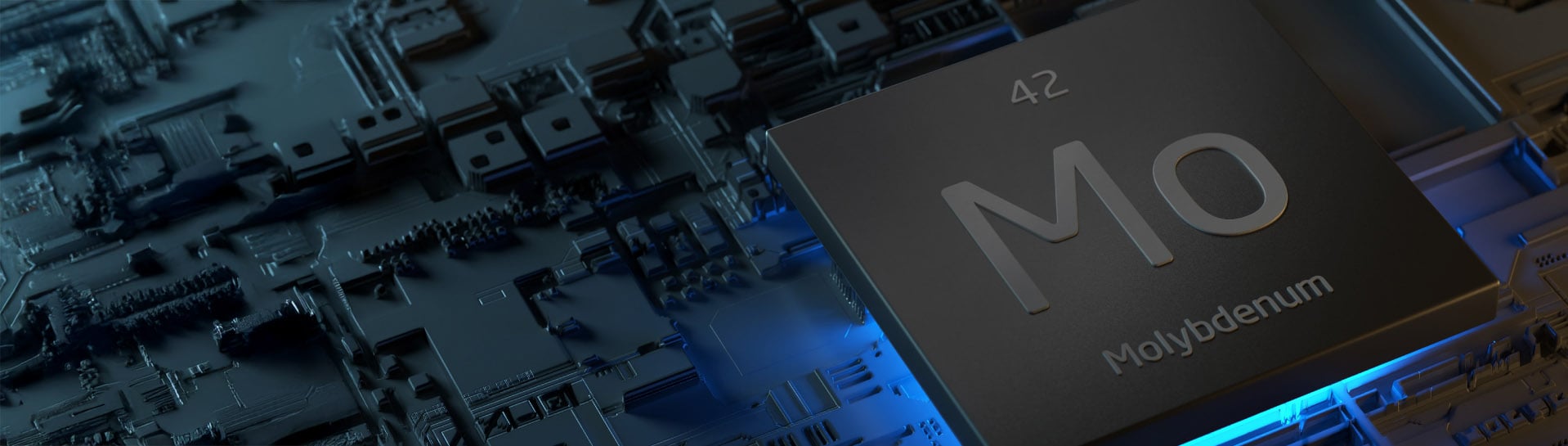
Molybdenum’s Role in Ultra-Fast Computing: The Metal Behind the Speed As the world races toward fast...

Science that is transforming lives and enabling the future
Molybdenum’s Role in Ultra-Fast Computing: The Metal Behind the Speed As the world races toward faster, smarter, and more connected technologies, the demand for ultra-fast computing is reshaping the semiconductor landscape. From AI and autonomous systems to 5G and edge computing, modern applications are generating massive volumes of data that must be processed, transmitted, and stored with unprecedented speed and reliability.
Effect of POU Filter Pore Size on EUV Bridge Defect Density
Hydrogen Halides in Semiconductor Manufacturing: Three Gases, Three Distinct Challenges and Solutions
Discover EDM-C3® Premium Copper-Impregnated Graphite In a previous discussion, we examined EDM-AF5®, a reliable graphite grade known for its balanced performance in electrical discharge machining (EDM). For applications requiring fine detail, challenging workpiece materials, and demanding machining conditions, EDM-C3® offers another level of capability.
End-to-End Manufacturing Excellence: Seven Questions Every New (or Growing) Fab Team Should Be Asking
Under Pressure: Solving High Viscosity Material Challenges in Advanced Packaging
Cleaner Chemistry and Faster Startup with Next Generation Ancillary Photochemical Filters
Solving Bridge Defects in EUV CAR Resists with Advanced UPE Filtration
Building Resilient Infrastructure to Better Serve Our Customers: A Vision from Abhijeet Bhandare “Our digital transformation is about one thing: being the most reliable, innovative partner for our customers.” – Abhijeet Bhandare
Collaborating to Solve Advanced Packaging Substrate Warpage, Thickness, and Heavy Payload Transport and Shipping Defect Challenges
Airborne molecular contamination (AMC) threatens semiconductor yield and reliability. Learn how Entegris helps fabs detect and control AMC with advanced filtration and data-driven strategies.
Optimizing Wafer Polishing: Innovations in CMP Slurry Characterization and Filtration
Molybdenum’s Role in Ultra-Fast Computing: The Metal Behind the Speed As the world races toward fast...

Effect of POU Filter Pore Size on EUV Bridge Defect Density

Hydrogen Halides in Semiconductor Manufacturing: Three Gases, Three Distinct Challenges and Solution...
Discover EDM-C3® Premium Copper-Impregnated Graphite In a previous discussion, we examined EDM-AF5®,...
End-to-End Manufacturing Excellence: Seven Questions Every New (or Growing) Fab Team Should Be Askin...

Under Pressure: Solving High Viscosity Material Challenges in Advanced Packaging

Cleaner Chemistry and Faster Startup with Next Generation Ancillary Photochemical Filters

Solving Bridge Defects in EUV CAR Resists with Advanced UPE Filtration

Building Resilient Infrastructure to Better Serve Our Customers: A Vision from Abhijeet Bhandare “Ou...

Collaborating to Solve Advanced Packaging Substrate Warpage, Thickness, and Heavy Payload Transport ...

Airborne molecular contamination (AMC) threatens semiconductor yield and reliability. Learn how Ente...

Optimizing Wafer Polishing: Innovations in CMP Slurry Characterization and Filtration
© 2026 Entegris. All Rights Reserved

